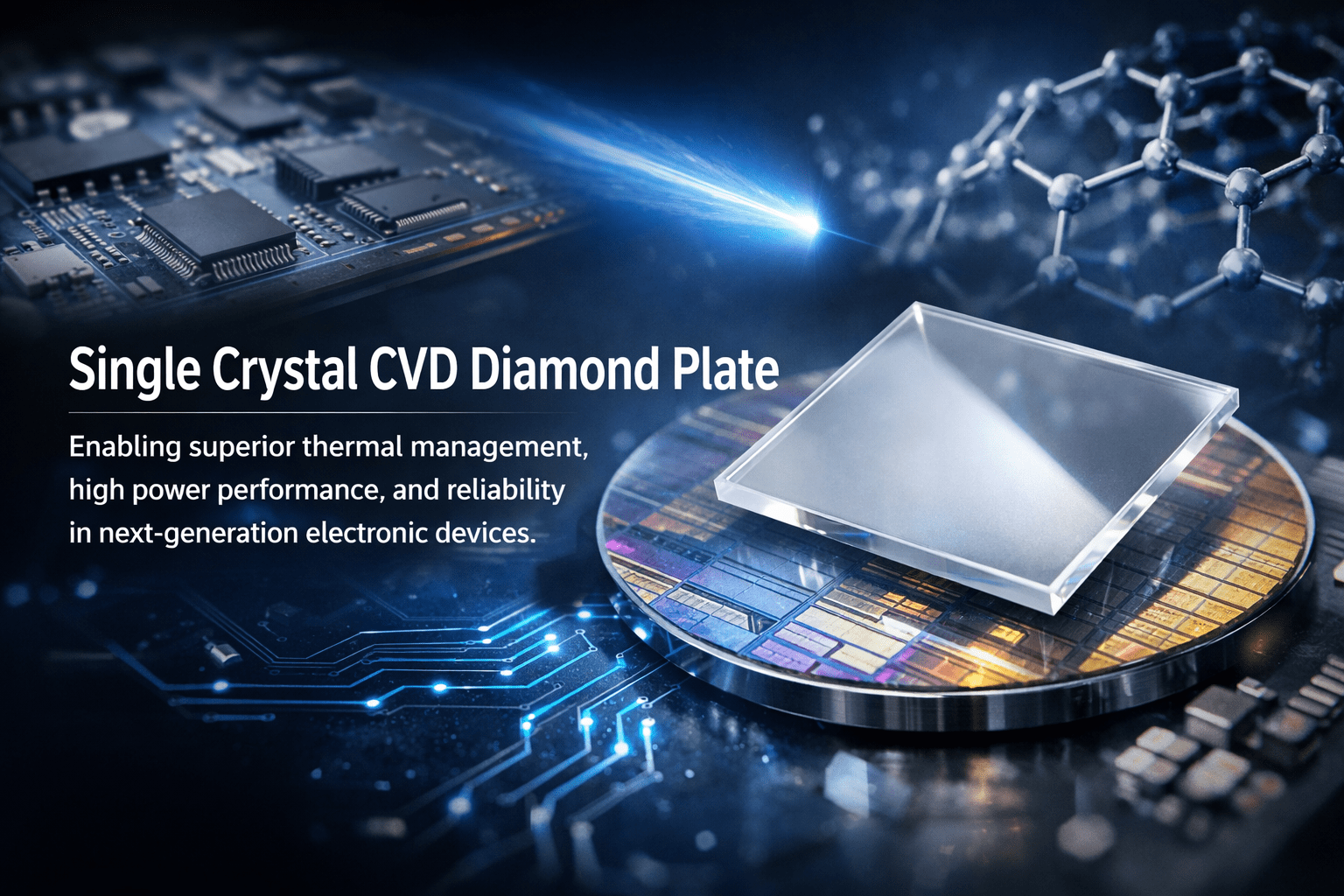
What Is a Single Crystal CVD Diamond Plate and Why It Matters in Advanced Electronics?
Understanding Single Crystal CVD Diamond Plates
A Single Crystal CVD Diamond Plate is a flat, precisely engineered diamond substrate grown atom by atom using the Chemical Vapor Deposition (CVD) process. Unlike natural diamonds or polycrystalline diamond films, this material has a continuous, uninterrupted crystal lattice across the entire plate.
Key Characteristics
- Single crystal structure (no grain boundaries)
- Ultra-high purity (extremely low nitrogen and boron levels)
- Controlled crystallographic orientation (typically (100) or (111))
- Exceptional surface finish (sub-nanometer roughness possible)
These attributes make single crystal CVD diamond fundamentally different from conventional diamond coatings and far more suitable for electronic and semiconductor applications.
How Single Crystal CVD Diamond Plates Are Made
The production of a single crystal diamond plate begins with a diamond seed crystal, usually oriented along a specific crystallographic plane such as (100). This seed is placed inside a CVD reactor.
Step-by-Step Process
- 1) Gas Activation
A mixture of hydrogen and methane is introduced into the reactor. - 2) Plasma Generation
Microwave or hot-filament energy breaks the gas molecules into reactive carbon radicals. - 3) Epitaxial Growth
Carbon atoms deposit on the diamond seed, continuing the same crystal lattice without forming defects. - 4) Thickness Build-Up
Over time, layers accumulate to form a diamond plate, ranging from tens of microns to several millimeters thick. - 5) Polishing & Finishing
The plate is laser cut, lapped, and polished to achieve ultra-smooth surfaces suitable for device fabrication.
The result is a synthetic diamond plate with properties superior to most natural diamonds and far more consistent from batch to batch.
Why Diamond Is Special for Electronics?
Diamond is not just “hard” it possesses a combination of physical properties unmatched by any other bulk material.
Exceptional Material Properties
- Thermal Conductivity: Up to 2000–2200 W/m·K (5× copper)
- Wide Bandgap: ~5.5 eV
- High Breakdown Field: ~10 MV/cm
- Low Dielectric Loss
- High Carrier Mobility
- Radiation Hardness
- Chemical Inertness
When these properties are realized in a single crystal form, they become transformative for electronics.
The Thermal Management Revolution
Heat is the silent performance killer in modern electronics. As power densities increase, even small thermal inefficiencies can lead to:
- Reduced performance
- Shortened device lifespan
- Thermal runaway
- Packaging failures
Why Single Crystal Diamond Plates Excel
- Ultra-fast heat spreading from hot spots
- Minimal thermal resistance
- Stable performance over wide temperature ranges
- Excellent CTE match with advanced semiconductor materials
This makes single crystal CVD diamond plates ideal as heat spreaders, substrates, and interposers in high-power electronics.
Enabling High-Power and High-Frequency Electronics
Advanced electronics such as RF amplifiers, power converters, and radar systems demand materials that can operate at:
- Higher voltages
- Higher frequencies
- Higher temperatures
Single crystal CVD diamond enables:
- Higher power density in GaN devices
- Improved RF efficiency
- Reduced thermal degradation
- Smaller, lighter system designs
This is particularly important for 5G/6G infrastructure, satellite communications, defense systems, and aerospace electronics.
Single Crystal Diamond in GaN-on-Diamond Technology
One of the most important applications today is GaN-on-Diamond.
Gallium Nitride (GaN) is a high-performance semiconductor but generates intense heat. By bonding GaN devices directly onto single crystal diamond plates:
- Heat is extracted directly from the active region
- Power output increases significantly
- Device reliability improves dramatically
This combination is rapidly becoming the gold standard for next-generation RF and power devices.
Quantum, Photonics, and Optical Applications
Beyond classical electronics, single crystal CVD diamond plays a vital role in emerging technologies.
Quantum Technologies
- Hosts stable NV⁰ and NV⁻ centers
- Enables quantum sensing and qubits
- Extremely low noise and long coherence times
Photonics & Optics
- Ultra-low optical absorption
- High transparency across wide wavelengths
- Ideal for high-power laser windows and photonic devices
These applications demand defect-free, ultra-pure single crystal diamond, something only advanced CVD processes can deliver.
Conclusion
A Single Crystal CVD Diamond Plate is far more than an exotic material. It is a core enabling technology for the future of electronics, power devices, photonics, and quantum systems. By combining unmatched thermal performance, electrical stability, and structural perfection, single crystal diamond is redefining what engineers can design—and what electronics can achieve. As manufacturing scales and adoption grows, expect single crystal CVD diamond plates to move from cutting-edge research labs into mainstream advanced electronic systems worldwide.