Global Market Outlook for Diamond Semiconductor Materials Through 2030
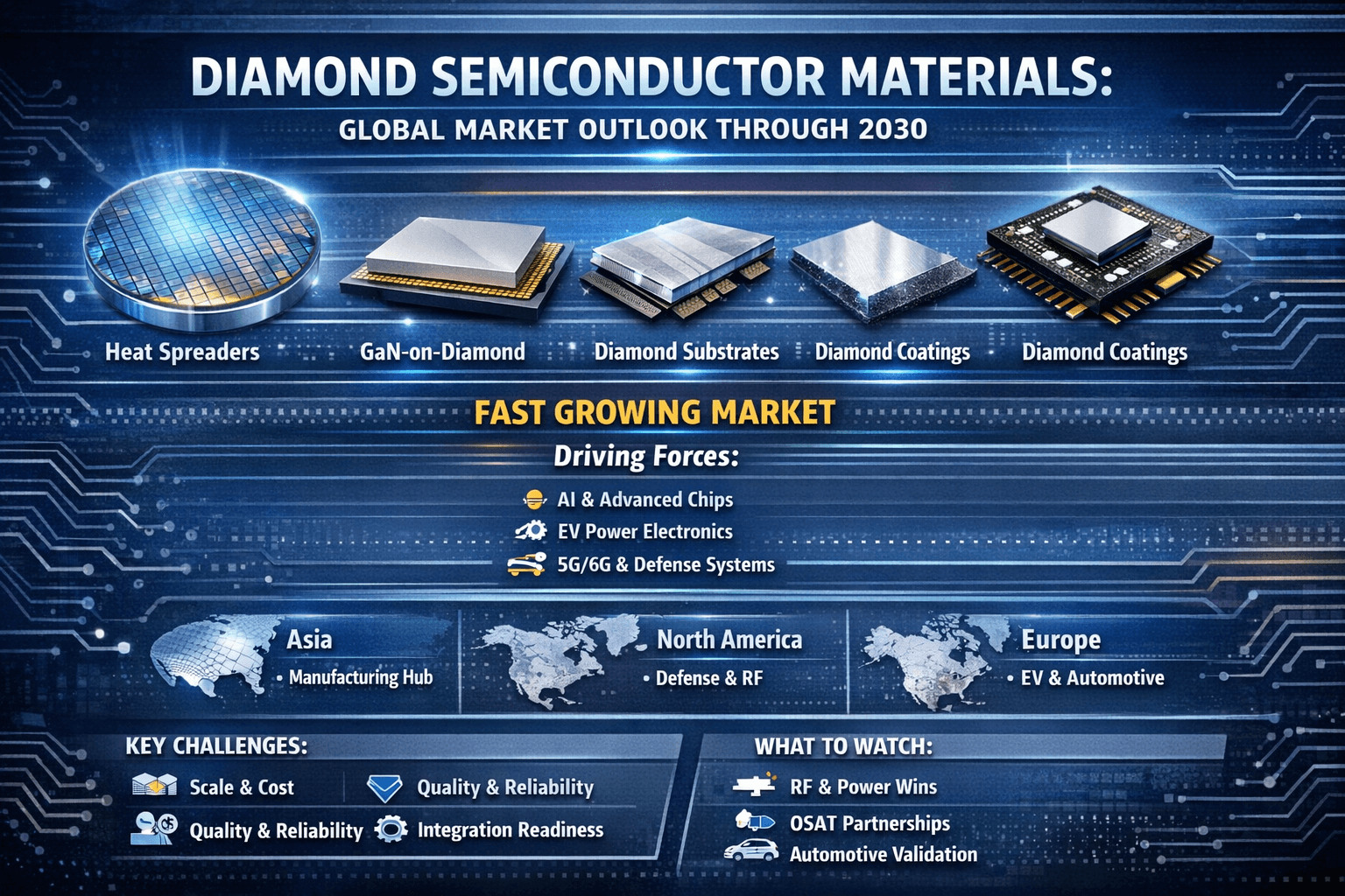
This blog summarizes what the market is expected to look like through 2030, what’s driving adoption, where the strongest demand is emerging, and what buyers and suppliers should watch closely.
1) What counts as “diamond semiconductor materials”?
When people say “diamond semiconductor materials,” they often mean a few related (but different) categories:
- Electronic-grade CVD diamond substrates / wafers (single-crystal or high-quality polycrystalline)
- CVD diamond heat spreaders / heat sinks (standalone parts or integrated into packages)
- Diamond coatings and diamond-based layers (including approaches that grow diamond closer to the active device region)
- GaN-on-diamond substrate stacks (diamond used as the thermal pathway beneath GaN devices)
These segments overlap, but the go-to-market and customer profiles can be very different (OSAT/packaging vs. device makers vs. RF/power module suppliers).
2) Market size: small today, growing fast (and forecasts vary)
Because this is still an emerging materials market, published numbers differ depending on definition and scope (pure “diamond semiconductors” vs. “diamond substrates” vs. “diamond heat spreaders” vs. broader synthetic diamond).
A few reference points from recent market reports:
- Diamond heat spreaders: one forecast estimates the segment growing from ~USD 0.35B (2025) to ~USD 0.56B (2030).
- Diamond semiconductor substrates: one forecast projects the market reaching ~USD 305.7M by 2030 (with a stated CAGR for 2024–2030).
- Diamond-based semiconductors (narrower definition): one widely circulated estimate projects growth from ~USD 61M (2024) to ~USD 139.1M (2030).
- GaN-on-diamond substrates: one forecast (2022–2031) places the category at ~USD 142M by 2031 with a mid-to-high teens CAGR.
How to interpret this:
- If you define the market as “diamond used in thermal management inside advanced electronics”, the number is larger (because it includes heat spreaders, package-level parts, and related materials).
- If you define it as “diamond as an active semiconductor or diamond wafers for devices”, it’s smaller but can show high percentage growth.
Either way, most outlooks point to the same conclusion: the category grows meaningfully by 2030, driven by thermal limits in AI compute, RF, EV power electronics, and advanced packaging.
3) Why demand is accelerating now?
A) Heat density is becoming the bottleneck in advanced chips
Transistor counts and 3D integration trends are pushing hotspot temperatures into ranges where traditional thermal stacks struggle. Recent research attention has also increased around growing/placing diamond closer to the device to reduce thermal resistance at the source of heat.
B) EVs, fast charging, and power conversion keep raising the bar
EV power semiconductor demand is expected to be very large by 2030 (with SiC growth often cited as the near-term driver), and diamond is increasingly discussed as a potential step-change thermal enabler for next-generation power electronics.
C) RF & high-frequency systems punish poor thermal performance
5G/6G infrastructure, radar, aerospace, and defense systems often accept higher material costs if it buys power handling and reliability. That makes diamond-based thermal paths compelling.
4) Where the money will be by 2030: segment-by-segment view
1) Heat spreaders & package-level thermal parts (near-term volume)
This is the most “commercial-ready” route because it can slot into established packaging supply chains. Many buyers here are looking for:
- predictable thermal performance
- thickness/flatness control
- metallization / attach compatibility
- scalable quality & supply assurance
This is also why heat spreaders show up with relatively larger 2030 numbers in market reports.
2) GaN-on-diamond (high-growth specialist segment)
GaN-on-diamond is especially attractive for RF power because it attacks one of GaN’s core limits: removing heat from the channel region. Forecasts commonly model this segment at high CAGR into the early 2030s.
3) Electronic-grade diamond substrates/wafers (strategic, longer adoption curve)
This segment is crucial for the long-term story, but it tends to be slower because:
- device ecosystems take time (tools, defect control, repeatability)
- customers need qualification cycles
- manufacturing scale-up is hard
Still, multiple forecasts show meaningful expansion by 2030 for “diamond substrate” definitions.
5) Regional outlook through 2030
Asia (manufacturing gravity)
- Packaging and assembly concentration makes Asia a key demand center for heat spreaders and thermal stack components.
- As advanced packaging ramps, supply chains that can deliver consistent diamond parts at scale will benefit.
North America (defense, RF, R&D, high-performance computing)
- Strong pull from aerospace/defense and research-driven programs.
- High willingness to pay for performance improvements.
Europe (automotive power electronics + industrial)
- Europe’s automotive ecosystem keeps demand strong for improved thermal solutions, especially as EV platforms mature.
6) Constraints that will shape the market (and winners)
Even with strong demand signals, several constraints will decide who wins between now and 2030:
Supply scalability & repeatability
Customers will ask:
- Can you deliver the same performance every batch?
- Can you ramp volume without yield collapse?
Cost-down curves
Diamond is often “worth it” when it removes the need for
- oversized heatsinks
- complex liquid cooling
- derating performance
- early failures / warranty costs
But cost-down still matters, especially for automotive.
Integration readiness
Diamond has to “fit” into customer processes:
- attach layers / metallization systems
- CTE/warpage management
- reliability under cycling
- inspection / traceability expectations
7) What to watch between now and 2030
Here are the signals that typically indicate the market is moving from “pilot” to “scaled adoption”:
- More public design wins in RF power and advanced packages
- OSAT + thermal material partnerships (diamond integrated as a standard option)
- Qualification milestones (automotive-grade validation, long reliability datasets)
- Process breakthroughs that enable diamond closer to the active device region (reducing hotspot temperatures materially)
8) Practical takeaways for buyers and decision-makers
If you’re evaluating diamond semiconductor materials for roadmaps through 2030:
1) Start with the problem statement: hotspot temperature, thermal resistance, and reliability
2) Decide if you need:
- package-level heat spreading (fastest path), or
- substrate/device-level innovation (bigger leap, longer cycle)
3) Build an evaluation plan around:
- thermal testing methodology
- attach process compatibility
- cycling reliability
- supply continuity & QA documentation