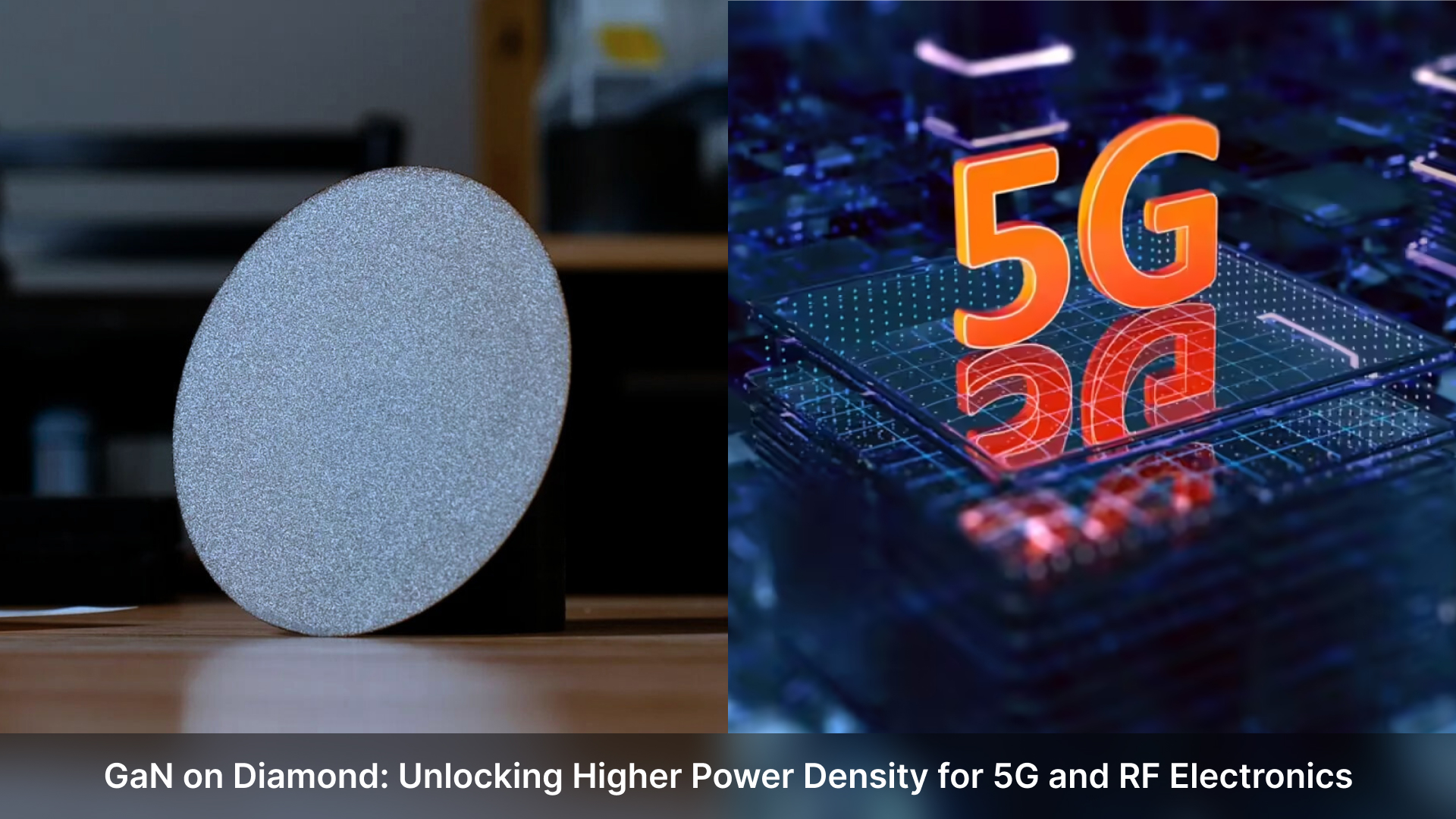
GaN on Diamond: Unlocking Higher Power Density for 5G and RF Electronics
The GaN Revolution and Its Thermal Limits
Gallium nitride transformed RF electronics when it entered commercial production in the early 2000s. Unlike silicon or even gallium arsenide (GaAs), GaN operates efficiently at high voltages, temperatures, and frequencies simultaneously. This trifecta enables power amplifiers that are smaller, more efficient, and more powerful than anything previously available critical advantages for applications from cellular base stations to military radar systems.
Traditional GaN devices use silicon carbide (SiC) or silicon substrates. SiC offers reasonable thermal conductivity around 400-500 W/mK, significantly better than silicon's 150 W/mK. This made SiC the preferred substrate for high-power GaN applications, enabling power densities reaching 5-10 watts per millimeter of gate width in typical operating conditions.
However, as 5G networks demand higher frequencies, greater bandwidth, and more sophisticated beam-forming capabilities, these power density figures prove insufficient. Next-generation systems require 15-30 watts per millimeter or more. At these extremes, even SiC substrates create thermal bottlenecks. The GaN active layer operates at junction temperatures approaching 200-250°C, limiting reliability and forcing designers to reduce power density or increase device size both undesirable compromises in space-constrained, cost-sensitive applications.
The fundamental issue is straightforward: heat generated in the thin GaN channel layer must travel through the substrate to reach the heat sink. With SiC substrates typically 100-150 micrometers thick, thermal resistance becomes substantial. The temperature differential between the GaN channel and the package backside can exceed 100°C, forcing conservative operating limits that leave performance on the table.
Why Diamond Changes Everything?
Diamond's thermal conductivity exceeding 2,000 W/mK is four to five times higher than SiC, but the benefits manifest more dramatically than this ratio suggests. When GaN is grown or bonded directly onto diamond substrates, the thermal resistance from the active channel to the heat sink decreases by 3-4x compared to GaN-on-SiC structures. This dramatic reduction enables revolutionary improvements across multiple performance dimensions.
First, junction temperatures drop by 50-100°C at equivalent power densities, dramatically improving reliability. Semiconductor failure rates follow Arrhenius relationships, where small temperature reductions yield exponential improvements in mean time to failure (MTTF). Operating a GaN device at 150°C instead of 200°C can increase lifespan from 10,000 hours to 100,000 hours or more transforming reliability economics for expensive infrastructure installations.
Second, the improved thermal management enables significantly higher power densities. With diamond substrates, GaN devices routinely achieve 20-30 W/mm in continuous operation, with experimental devices demonstrating beyond 40 W/mm. This allows smaller amplifiers delivering equivalent power, reducing size, weight, and cost particularly valuable in aerospace and defense applications where every gram matters.
Third, thermal performance improvements enable better efficiency at higher frequencies. GaN-on-diamond devices maintain high power-added efficiency (PAE) at millimeter-wave frequencies where GaN-on-SiC devices struggle. For 5G applications operating at 28 GHz, 39 GHz, or higher mmWave bands, this efficiency advantage directly impacts network economics through reduced energy consumption and cooling requirements.
Fourth, diamond's thermal stability enables more aggressive designs. Engineers can pack transistors more densely, use higher bias voltages, and push operating points toward maximum performance without excessive thermal margin. This design freedom translates to superior system-level performance in bandwidth, linearity, and output power.
Manufacturing GaN-on-Diamond: From Lab to Production
Creating GaN-on-diamond structures presents significant technical challenges. You cannot simply grow GaN directly on diamond the lattice mismatch and thermal expansion differences would create catastrophic defects. Instead, manufacturers employ sophisticated wafer bonding or transfer processes.
The most common approach grows GaN on its native substrate or a compatible transition layer, then bonds this structure to a diamond substrate before removing the original substrate. Variations include growing GaN on SiC, bonding to diamond, then etching away the SiC; or growing GaN on silicon with transition layers, bonding to diamond, then removing the silicon. Each approach involves precise surface preparation, low-temperature bonding techniques, and careful substrate removal without damaging the delicate GaN epitaxial layers.
Surface quality proves critical even nanometer-scale imperfections at the GaN-diamond interface create thermal resistance that negates diamond's benefits. Advanced techniques use molecular bonding, where atomically clean surfaces form direct chemical bonds without intermediate adhesive layers. Achieving consistent, low thermal boundary resistance (TBR) across production wafers remains a key challenge and differentiator among manufacturers.
Several companies have developed commercial GaN-on-diamond processes. Akash Systems, a US-based startup, pioneered volume production using proprietary bonding techniques. Element Six and II-VI Corporation provide diamond substrates specifically engineered for GaN integration. Traditional GaN manufacturers like Qorvo and Wolfspeed are developing their own GaN-on-diamond capabilities, recognizing the technology's strategic importance.
Recent manufacturing advances have improved yields and reduced costs substantially. While GaN-on-diamond wafers remain 2-4x more expensive than GaN-on-SiC equivalents, the performance advantages often justify the premium for demanding applications. As production scales and processes mature, cost premiums continue declining, accelerating adoption.
5G Infrastructure: The Killer Application
Massive MIMO (multiple-input, multiple-output) base stations represent GaN-on-diamond's most compelling near-term application. These systems employ dozens or hundreds of power amplifiers working in concert to create directed beams toward individual users, dramatically improving network capacity and coverage. Each amplifier must deliver 10-40 watts efficiently in compact form factors suitable for dense antenna arrays.
Traditional GaN-on-SiC amplifiers work but require substantial cooling infrastructure, adding size, weight, and cost to antenna installations. In dense urban deployments where equipment must mount on streetlights or building facades, size and weight constraints are severe. GaN-on-diamond enables smaller, lighter amplifiers that simplify installation and reduce structural requirements.
Energy efficiency matters enormously at scale. A typical urban 5G deployment might include thousands of base stations, each running continuously. Improving amplifier efficiency by 5-10% through better thermal management translates to megawatts of reduced power consumption across a network significant operational savings and environmental benefits. Mobile network operators are intensely interested in any technology that improves performance while reducing total cost of ownership.
The shift to millimeter-wave 5G frequencies (above 24 GHz) makes GaN-on-diamond even more valuable. At these frequencies, thermal effects degrade performance more severely, and GaN-on-SiC devices struggle to maintain efficiency. GaN-on-diamond devices demonstrate superior linearity and efficiency at mmWave frequencies, enabling the high-bandwidth applications that 5G promises but that require these challenging frequency bands.
Defense and Aerospace Applications
Military radar, electronic warfare, and satellite communications systems push power density requirements even further than commercial 5G. Active electronically scanned array (AESA) radars for fighter aircraft might pack thousands of GaN transmit/receive modules into conformal antenna installations where cooling options are extremely limited. GaN-on-diamond's thermal advantages are essentially mandatory for next-generation systems.
Space applications face unique thermal challenges heat rejection in vacuum relies solely on radiation, making thermal management exponentially more difficult. GaN-on-diamond satellite transponders and phased array antennas enable higher power output in mass-constrained spacecraft, improving communications bandwidth and radar performance. Several satellite manufacturers have publicly disclosed GaN-on-diamond usage in next-generation constellations.
Defense programs often accept higher component costs for performance advantages, making these applications early adopters that drive manufacturing maturity. The RF power module in Raytheon's GaN-based AESA radars reportedly uses diamond thermal management, though specific implementations remain classified. As these defense-funded technologies mature and manufacturing scales, costs decline toward levels acceptable for commercial applications.
Remaining Challenges and Future Outlook
Despite remarkable progress, GaN-on-diamond faces ongoing challenges. Cost remains the primary barrier to mass adoption diamond substrates add $50-200 per chip depending on size and quality, significant for price-sensitive commercial markets. However, the economic calculation improves as system-level benefits (smaller amplifiers, reduced cooling, improved reliability) offset component costs.
Thermal boundary resistance between GaN and diamond continues limiting performance below theoretical levels. Even excellent bonding processes create interfacial thermal resistance of 10-20 m²K/GW, which at extreme power densities creates meaningful temperature rise. Research into nanostructured interfaces, graphene intermediate layers, and advanced surface treatments aims to reduce TBR toward 5 m²K/GW or below, further unleashing diamond's potential.
Manufacturing yield and consistency require continued improvement. Wafer-scale bonding processes must achieve uniform thermal performance across entire wafers while maintaining electrical properties and mechanical reliability through thermal cycling and operational stress. As processes mature, these challenges are steadily being overcome.
The trajectory is unmistakable: GaN-on-diamond is transitioning from exotic research topic to production reality. Market analysts project the GaN-on-diamond RF device market growing from roughly $50 million in 2024 to over $500 million by 2030, driven primarily by 5G infrastructure and defense applications. As 6G research accelerates and terahertz systems emerge, the thermal advantages of diamond substrates become even more essential.
For RF engineers designing tomorrow's communications and radar systems, GaN-on-diamond represents not merely an incremental improvement but a fundamental capability enabler. The technology unlocks power densities, efficiencies, and form factors impossible with conventional approaches, making the previously impossible not just possible, but practical. In the race to deliver ever-higher bandwidth, ever-greater range, and ever-smaller systems, diamond isn't just an advantage—it's becoming the foundation upon which next-generation RF electronics must be built.