Diamond Semiconductors vs SiC and GaN: Who Wins the Future of High Power Electronics?
The Material Properties Showdown
Understanding this competition requires examining fundamental material properties. Silicon's 1.1 eV bandgap limited its operating voltage and temperature, prompting the search for wide-bandgap alternatives. SiC delivers 3.3 eV, GaN offers 3.4 eV, and diamond boasts an extraordinary 5.5 eV bandgap the widest of any semiconductor.
This bandgap advantage translates directly to performance. Diamond's breakdown field strength exceeds 10 MV/cm compared to SiC's 2.5 MV/cm and GaN's 3.3 MV/cm. Higher breakdown fields enable thinner drift layers in power devices, dramatically reducing on-resistance and conduction losses. Diamond's electron mobility (2,200 cm²/V•s) and hole mobility (1,800 cm²/V•s) exceed SiC's values, enabling faster switching with lower losses.
Thermal properties tell an even more dramatic story. Diamond's thermal conductivity exceeds 2,000 W/mK five times SiC's 400 W/mK and twenty times GaN's 130 W/mK. This extraordinary heat dissipation enables diamond devices to operate at extreme power densities without sophisticated cooling infrastructure. Diamond maintains semiconductor functionality beyond 500°C, far exceeding SiC's 600°C junction temperature limit and GaN's more modest thermal tolerance.
Theoretically, diamond power devices could achieve switching losses one-tenth those of SiC equivalents, operate at junction temperatures exceeding 300°C without degradation, handle voltages beyond 30 kV in compact form factors, and eliminate cooling requirements in many applications. These aren't incremental improvements they're transformative capabilities that would revolutionize power electronics architecture.
The SiC Success Story
Silicon carbide has transitioned from laboratory curiosity to multi-billion-dollar industry over the past two decades. Companies like Wolfspeed, Rohm, and STMicroelectronics produce commercial SiC MOSFETs and Schottky diodes serving automotive, industrial, and renewable energy markets. Tesla's Model 3 famously adopted SiC inverters, validating the technology for mass-market EVs and triggering industry-wide adoption.
SiC's success stems from manufacturing maturity. While wafer quality isn't perfect defect densities remain higher than silicon it's sufficient for commercial production at acceptable yields. Six-inch wafers are standard, with eight-inch production emerging. Processing equipment adapted from silicon foundries enables relatively straightforward device fabrication. Most importantly, SiC devices demonstrate proven reliability in demanding applications, accumulating millions of operational hours validating long-term performance.
The economics increasingly favor SiC. Although SiC devices cost 2-3x more than silicon equivalents, system-level benefits reduced cooling requirements, higher switching frequencies enabling smaller passive components, improved efficiency reducing energy costs deliver compelling total cost of ownership. As production scales, SiC device costs continue declining while performance improves through incremental process optimization.
For electric vehicles, SiC enables 5-10% range improvements through efficiency gains and power electronics miniaturization. For solar inverters and grid infrastructure, SiC reduces size, weight, and losses while improving power density. The market opportunity is enormous analysts project SiC power semiconductor revenue reaching $8-12 billion by 2030.
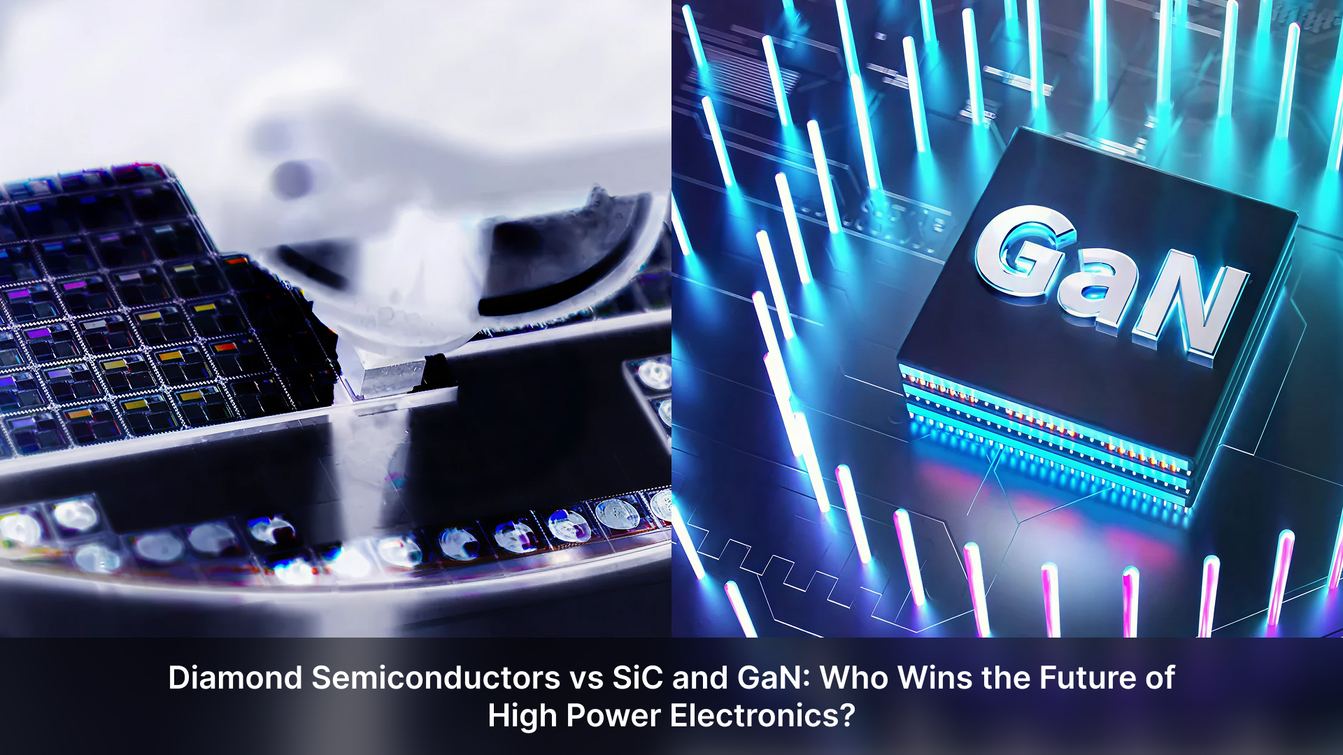
GaN's Rapid Ascent
Gallium nitride pursued a different trajectory, initially targeting RF and microwave applications before expanding into power electronics. GaN's appeal lies in extremely fast switching capabilities and compatibility with lateral device structures on silicon substrates a crucial cost advantage.
GaN Systems, Navitas Semiconductor, and Efficient Power Conversion pioneered GaN power devices for applications from smartphone chargers to datacenter power supplies. GaN's high electron mobility and lateral HEMT (high electron mobility transistor) architecture enable switching frequencies beyond 1 MHz far exceeding SiC capabilities allowing dramatically smaller, lighter power converters.
Consumer electronics adoption drove rapid volume scaling. USB-C chargers using GaN achieve 65-100 watt output in packages one-third the size of silicon equivalents. Datacenter power supplies use GaN to improve efficiency while reducing footprint. Automotive systems increasingly adopt GaN for onboard chargers and DC-DC converters where high-frequency operation provides advantages.
GaN's substrate flexibility is a major advantage. While native GaN substrates enable optimal performance, growing GaN on silicon wafers dramatically reduces costs, leveraging existing semiconductor manufacturing infrastructure. This compromise accepts some performance degradation for economic viability a pragmatic choice accelerating commercialization.
The market dynamics favor GaN for mid-voltage (100-650V) applications requiring ultra-fast switching, while SiC dominates high-voltage (1,200V+) applications where blocking voltage and thermal performance matter most. This complementary positioning allows both technologies to thrive in distinct niches.
Diamond's Daunting Challenges
Despite superior material properties, diamond semiconductors face severe obstacles preventing commercialization. Substrate availability represents the primary barrier. High-quality single-crystal diamond wafers suitable for electronics cost $5,000-20,000 per small wafer orders of magnitude more than SiC or GaN. Chemical vapor deposition (CVD) growth is slow and expensive, with wafer sizes limited to two inches or smaller. Scaling to economically viable wafer sizes remains an unsolved challenge.
Doping proves extraordinarily difficult. Diamond's strong covalent bonding makes incorporating dopants challenging, and achieving both n-type and p-type doping with sufficient carrier concentrations and mobilities has frustrated researchers for decades. Boron doping for p-type diamond works reasonably well, but reliable n-type doping remains problematic. Without controllable doping, fabricating essential device structures like p-n junctions becomes impractical.
Contact resistance plagues diamond devices. Creating low-resistance ohmic contacts to diamond requires careful surface engineering and specific metal combinations. Even optimized contacts exhibit higher resistance than SiC or GaN equivalents, degrading device performance and partially negating diamond's material advantages.
Manufacturing infrastructure doesn't exist. Unlike SiC and GaN, which adapted silicon foundry equipment, diamond requires entirely new processing techniques, equipment, and expertise. The investment required to establish diamond semiconductor manufacturing at commercial scale would be billions of dollars without guaranteed returns.
Most critically, no compelling application justifies diamond's development costs given SiC and GaN's capabilities. While diamond offers superior properties, SiC and GaN already meet most application requirements at acceptable cost. The incremental performance gain from diamond doesn't justify order-of-magnitude cost increases for most markets.
Who Wins the Future?
The answer depends on timeframe. For the next 10-15 years, SiC and GaN will dominate high-power electronics. SiC owns high-voltage, high-power applications in automotive, industrial, and grid infrastructure. GaN dominates mid-voltage, high-frequency applications in consumer electronics, datacenter power, and RF systems. Both technologies continue improving through incremental advances while production scales drive costs down and market adoption accelerates.
Diamond remains a laboratory pursuit for now. Researchers continue making progress on substrate growth, doping techniques, and device fabrication, but commercial viability remains distant. Optimistic projections suggest limited commercial diamond devices might emerge around 2035-2040, likely targeting ultra-niche applications where extreme performance justifies extraordinary costs perhaps aerospace, defense, or specialized scientific instruments.
However, breakthrough developments could accelerate diamond's timeline. Revolutionary substrate growth techniques, novel doping approaches, or creative device architectures that circumvent current limitations might unlock practical diamond electronics sooner than expected. The potential rewards transformative performance enabling entirely new applications justify continued research investment even with uncertain commercialization prospects.
Conclusion
SiC and GaN have already won the near-term future of high-power electronics. Both technologies transitioned from research to commercial success, capturing growing markets worth tens of billions of dollars. They deliver compelling performance improvements over silicon at increasingly acceptable costs, satisfying current and foreseeable application requirements.
Diamond remains the ultimate semiconductor superior in nearly every measurable property. Yet superior materials don't always win markets. Manufacturing practicality, economic viability, and sufficient performance for real applications determine commercial success. Diamond's path to commercialization requires solving multiple fundamental challenges simultaneously, a daunting prospect given SiC and GaN's established momentum.
The future likely holds continued SiC and GaN dominance for decades, with diamond emerging eventually for ultra-specialized applications if manufacturing obstacles can be overcome. In semiconductors, as in life, perfection is expensive, and good enough often wins. For high-power electronics, SiC and GaN are more than good enough they're excellent. Diamond may be perfect, but perfect might not be necessary.